If you like experimenting with electronics sooner or later you’ll want to create an etched PCB with your own circuit. For testing purposes there’s of course the breadboard and simple circuits can be easily built on a stripboard but as soon as the complexity grows designing layouts in some electronics software is the natural way to go.
Although there are some manufacturers that offer professional PCBs at a reasonable price it is often much faster to make the prototype at home. But it takes some initial investment and work to set up a proper manufacturing process. Basically you’ll need two things (besides mechanical tools, e.g. a drill):
- Circuit transfer to your PCB
- Etching equipment
The etching is comparatively easy, it’s the circuit transfer to the PCB that’s more complicated. There are several methods to achieve this, for example: direct printing/plotting, toner transfer or lithography. My method of choice is lithography as it gives IMHO the best results and is actually quite easy and fast. PCBs with a photoresist on them can be bought off the shelf for little money, so what we need additionally is a way to make masks and an UV exposure unit. In the following I will show you a simple DIY exposure unit.
Always be careful when when working with mains voltage. If you are not experienced with don’t attempt this build!
Prerequisites
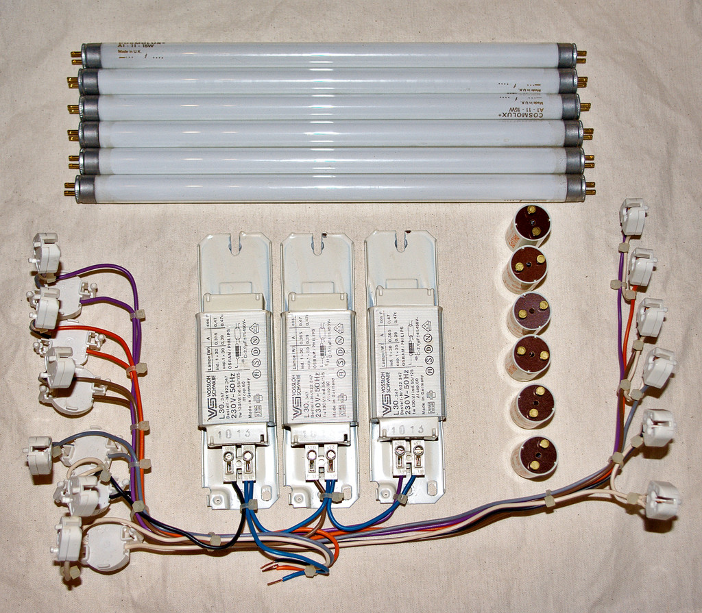
Commercial exposure units, even small ones, cost easily more than 100 € which is the reason I decided to build my own. There are plenty of instructions on the web which I took as an inspiration for my machine. This is a rough parts list:
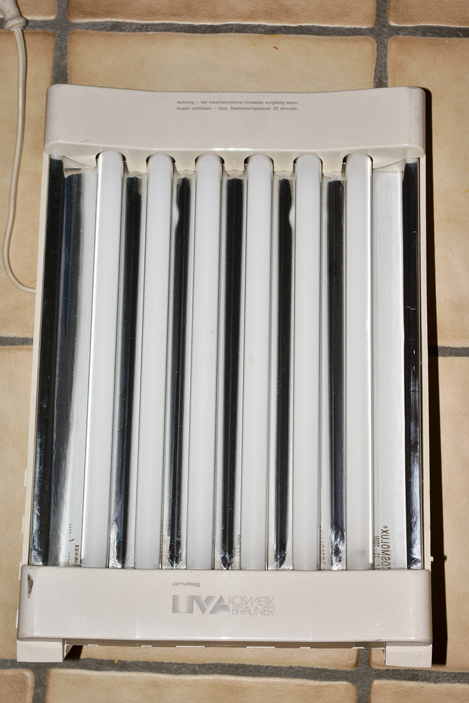
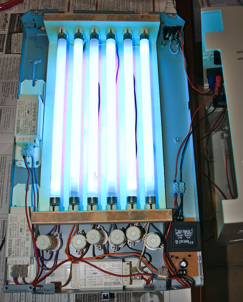
- Facial tanner (Price: < 10 €)
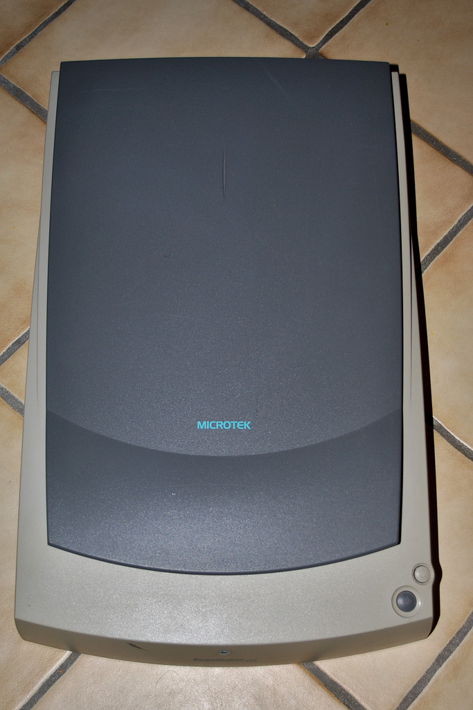
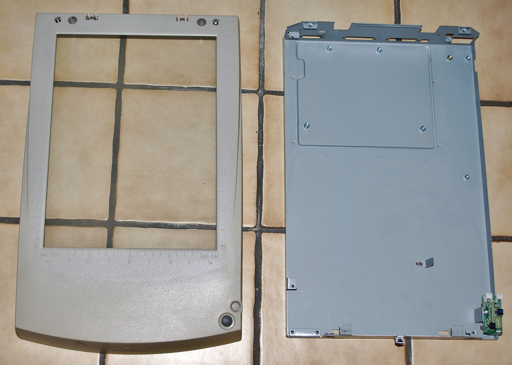
- Flatbed scanner (can be broken, doesn’t matter. Price: < 5 €)
- Plywood or something similar (Price: 1-2 €)
- Cables, fans, switch, connectors (e.g. luster terminals)
- Glue
The facial tanner provides the UV tubes and necessary ballasts while the scanner is salvaged for its casing including a glass plate to put your PCB on. I got my parts on eBay and a local hardware store for a total of about 35 €, give or take.
Putting things together
Once you get these parts you’ll have to construct some mounting box to put inside the scanner housing. Mine is made from cheap plywood where I drilled in mounting holes for the sockets. Additionally I added a 12 V DC power supply for the fans (transformer, 4 diodes and a capacitor). The lamps get pretty warm so you really want some kind of ventilation if it runs for extended periods. If you turn it on shortly you might well get away without any fans.
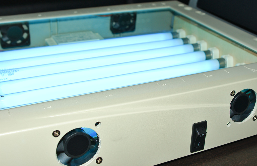
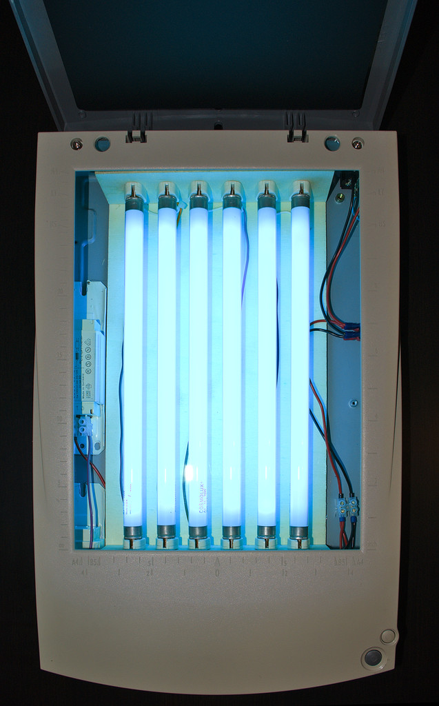
Here’s how the thing looks once everything is in place, although not yet wired up. The distance between the tubes was chosen to be identical to the distance between the tubes and the glass plate where you put your PCB. This gives a homogeneous distribution with maximum irradiance.
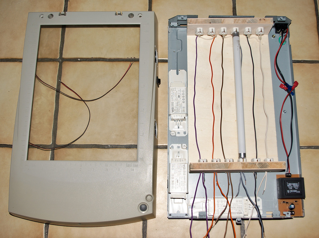
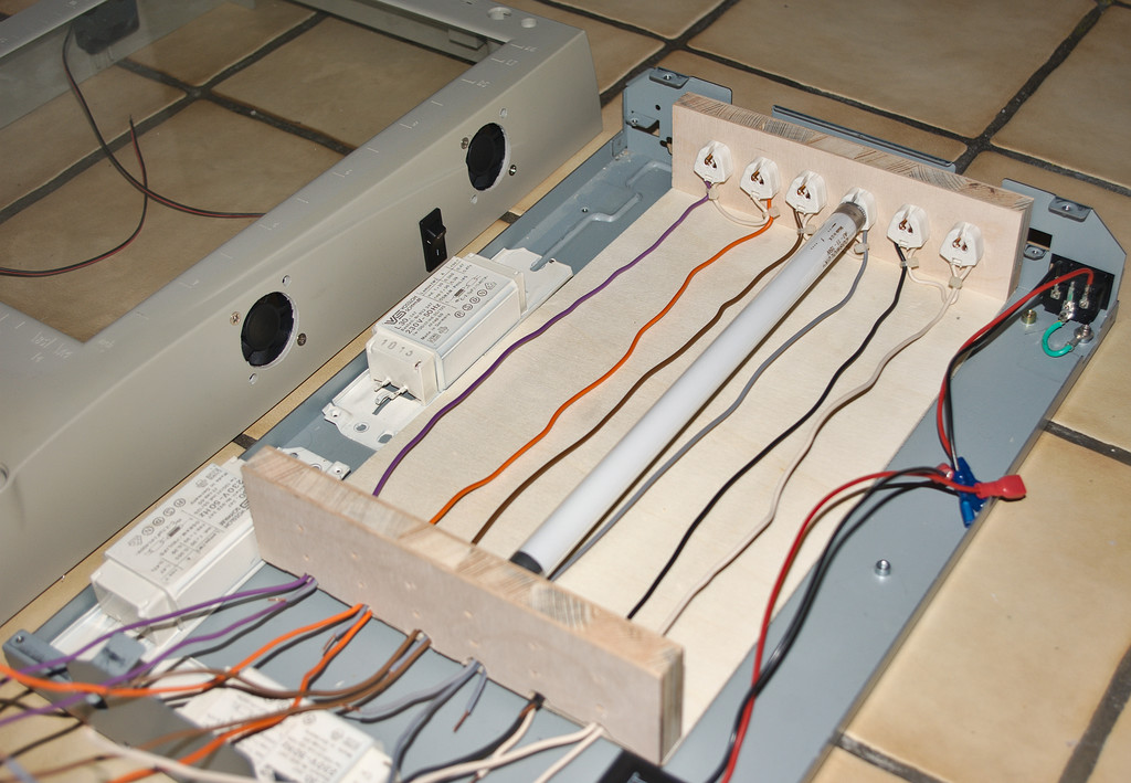
The last part is wiring everything up correctly and properly mount the parts inside the case. I used hot glue to fasten everything in place, works pretty well. Afterwards just close your case up and you’re done! Note that I did not add the reflective mirror from the original facial tanner in this unit. It didn’t fit in properly and after testing the exposure unit it proved to be powerful enough without this.
Commissioning
As next step you’ll need to find the right exposure time. Put multiple strips of black tape on a fresh PCB and taking one off every 15 seconds during the exposure. When you develop it you can directly see which strip is the first to dissolve completely. If you remembered the corresponding time, that’s your exposure time. For my machine I need to expose the photoresists for about 2 minutes (YMMV).
Happy etching! 😀